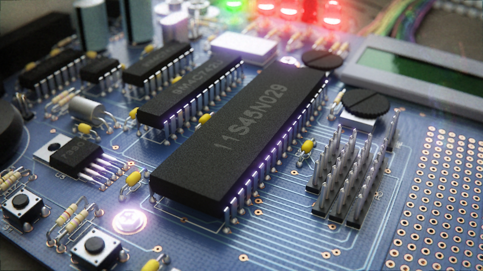
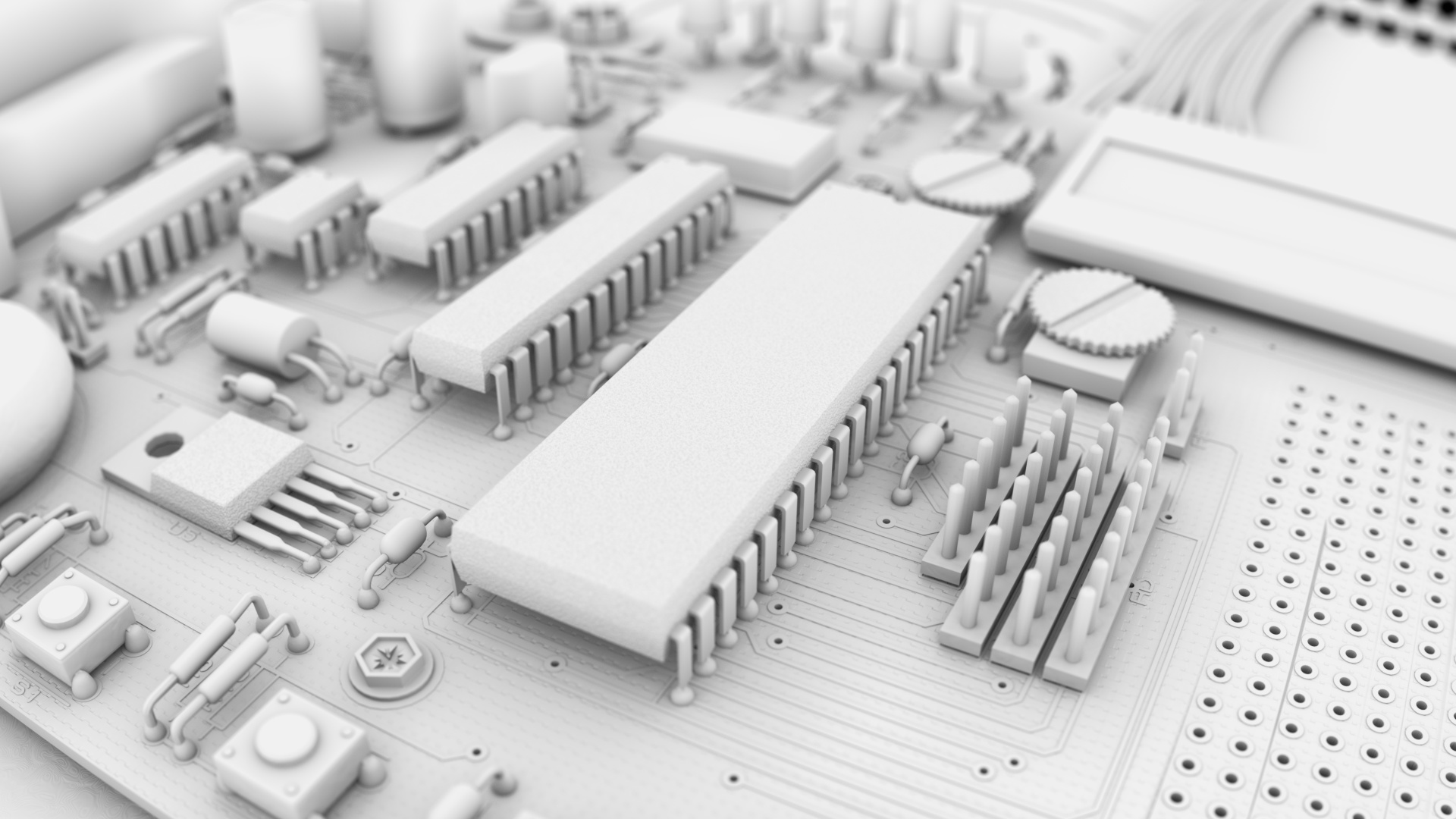
I used Isis Proteus for the board, then exported a 3DS model to blender and polished it and made all the materials and lighting and some additional modeling.
I tried to simulate a decent phone camera and I added all the small effects like dirty lens, “cubism” and noise, desaturation, purple-ish highlights, black contours on high contrast area, lower response to bright red light ( at least it’s how my phone’s camera reacts)
AO:
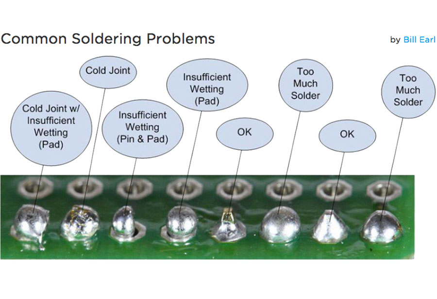
Those look like what we in the industry call “cold solder joints” boards are normally soldered from the other side and on this side the solder should look more like water that flowed over the surface, there should not be any bulbs of solder seen on this side (with the exception of the button thingies)
PCB boards may have a fiber glass weave inside of them but they should be perfectly smooth on top otherwise the copper traces would lift off far easier.
There are boards with one side and with two sides.
True, I should have made some research before. Thanks 
I like it! Well done!
Thank you
I’m a retired electronics tech, I quite well know that. But bulb like solder joints have too much solder and tend to be cold joints.
Nice model and texture and cool information joseph, didn’t know about that