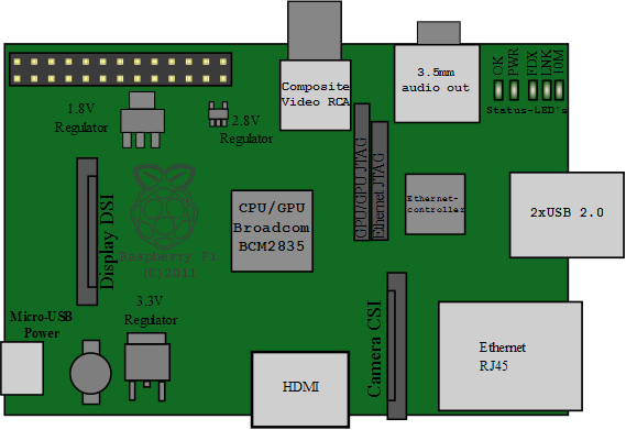
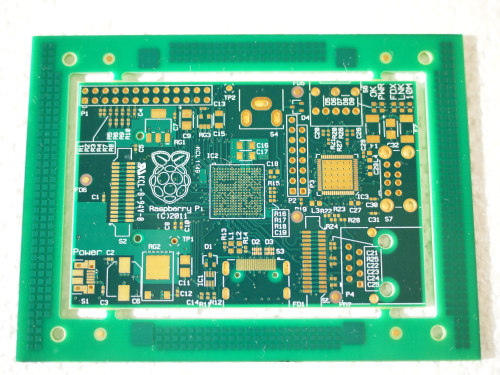
On PCB’s, things labelled with an “R” are almost always a resistor. If it’s between the ethernet jack and the LAN chip, it may be to do with impedance matching. It’s hard to explain impedance matching without getting technical, but if you imagine that you have a heavy object and a light object and they hit each other, the light object will go flying while the heavy object won’t move much. If you have a wire with high resistance and one with low resistance, then you can get some weird electrical effects (only a problem at high signal speeds such as high-speed-ethernet).
More useful that looking at the PCB layout is to find the schematic - unfortunately the Pi is not open source hardware, so you can’t actually get the schematic for recent models. Fortunatly, the LAN chip has a datasheet: http://ww1.microchip.com/downloads/en/DeviceDoc/00002304A.pdf
It doesn’t show the signal side, but it does show some of the requirements for the power supply schematics. If you are planning to implement a PCB with these components, be aware that high-speed PCB design is not trivial.